PCIe for hackers: our M.2 card is finished
We started designing a PCIe card last week, an M.2 dongle to dongle adapter, which adds an extra link to the dongle slot inside - useful for making full use of some rare but fancy dongle cards. Now the schematic is complete, component placement has been determined, and we only need to route the differential pairs - should be simple, right? Buckle up.
Make the Diffpairs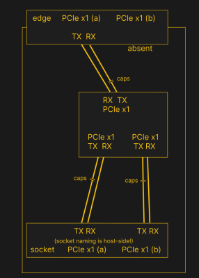 PCI We need TX pairs connected to RX at one other end, like UART - and that's non-negotiable. Connectors will use host side naming and vice versa. As shown in the diagram, we connect the TX of the socket to the RX of the chip and vice versa; if we ever get confused, the laptop schematic is here to help us clear things up. To summarize, just reverse the names on the link coming to the PCIe switch, since the PCIe switch acts as a device on the board; both switch links go to the E-key socket, and for the purposes of this socket, the PCIe switch acts as a host.
During the initial routing of this board, I absolutely forgot another important thing for the PCIe serial capacitors on each data pair, on the host TX side of the link. We need three pairs of capacitors here - on TX of the PCIe switch uplink and two pairs on the TX side of the switch - again, the naming is on the host side. I only remembered this after I finished routing all the diffpairs, and, after a bit of thinking, I decided this was my chance to try the 0201 capacitors. For that, I took fingerprints from [Christoph]'s wonderful project, called "Moon Phase Effect on Tombstoning" - with such a name, those fingerprints must be good.
We already talked about differential pair calculations in one of the PCIe articles, and there was also a demonstration video! That said, let's repeat the math on this one - I'll show how to go from "information on the PCB fabrication website" to "proper width and clearance differences", with some fun shortcuts. Our setup is, once again, to have signals on the outer layers, referenced to the layer on the ground just below them. Unfortunately, I don't yet understand how to calculate differential impedance for signal layers sandwiched between two ground planes, ie - if there are any commenters willing to share this knowledge, I would greatly appreciate your input! At this point, I don't see that there would be any tangible benefit to such an arrangement, anyway.
Different stacking might help
We started designing a PCIe card last week, an M.2 dongle to dongle adapter, which adds an extra link to the dongle slot inside - useful for making full use of some rare but fancy dongle cards. Now the schematic is complete, component placement has been determined, and we only need to route the differential pairs - should be simple, right? Buckle up.
Make the DiffpairsPCI We need TX pairs connected to RX at one other end, like UART - and that's non-negotiable. Connectors will use host side naming and vice versa. As shown in the diagram, we connect the TX of the socket to the RX of the chip and vice versa; if we ever get confused, the laptop schematic is here to help us clear things up. To summarize, just reverse the names on the link coming to the PCIe switch, since the PCIe switch acts as a device on the board; both switch links go to the E-key socket, and for the purposes of this socket, the PCIe switch acts as a host.
During the initial routing of this board, I absolutely forgot another important thing for the PCIe serial capacitors on each data pair, on the host TX side of the link. We need three pairs of capacitors here - on TX of the PCIe switch uplink and two pairs on the TX side of the switch - again, the naming is on the host side. I only remembered this after I finished routing all the diffpairs, and, after a bit of thinking, I decided this was my chance to try the 0201 capacitors. For that, I took fingerprints from [Christoph]'s wonderful project, called "Moon Phase Effect on Tombstoning" - with such a name, those fingerprints must be good.
We already talked about differential pair calculations in one of the PCIe articles, and there was also a demonstration video! That said, let's repeat the math on this one - I'll show how to go from "information on the PCB fabrication website" to "proper width and clearance differences", with some fun shortcuts. Our setup is, once again, to have signals on the outer layers, referenced to the layer on the ground just below them. Unfortunately, I don't yet understand how to calculate differential impedance for signal layers sandwiched between two ground planes, ie - if there are any commenters willing to share this knowledge, I would greatly appreciate your input! At this point, I don't see that there would be any tangible benefit to such an arrangement, anyway.
Different stacking might help
What's Your Reaction?