TSMC's long road from round to square silicon wafers
TSMC's long road from round to square silicon wafers
Crystal
of
Cultivated by Czochralski
silicon.
Most
of
We
will
probably
to have
seen
semiconductor
pads
as
they
trundle
their
path
through
A
chip
factory,
And
a few
of
We
can
to have
request
about
Why
they
are
round.
This
roundness
East
A
obvious
issue
When
A
considered
that
THE
chip
dies
themselves
are
rectangular,
meaning
that
A
significant
Rising
of
THE
dies
engraved
In
THE
pads
END
up
be
incomplete
And
Thus
as
waste,
especially
with
(Dear)
big
dies.
This
East
not
A
notion
which
has
escaped
THE
attention
of
chip
manufacturers
as
TSMC,
with
This
particular
maker
apparently
Currently
to study
A
path
has
TO DO
square
substrates
A
reality.
According to
has
THE
information
provided
has
Nikkei
Asia
by
people
with
direct
awareness,
Currently
510
mm
X
515
mm
substrates
are
be
tested
which
would be
replace
THE
current
standard
12″
(300
mm)
round
platelets.
For
massive
dies
such
as
NVidia
H200
(814
mm2),
This
means
that
approximately
three
times
as
a lot
would be
adjust
by
slice.
As
For
When
This
technology
will
go
In
production
East
unknown,
but
there
exist
significant
incentive
In
THE
current
walk
has
TO DO
he
work.
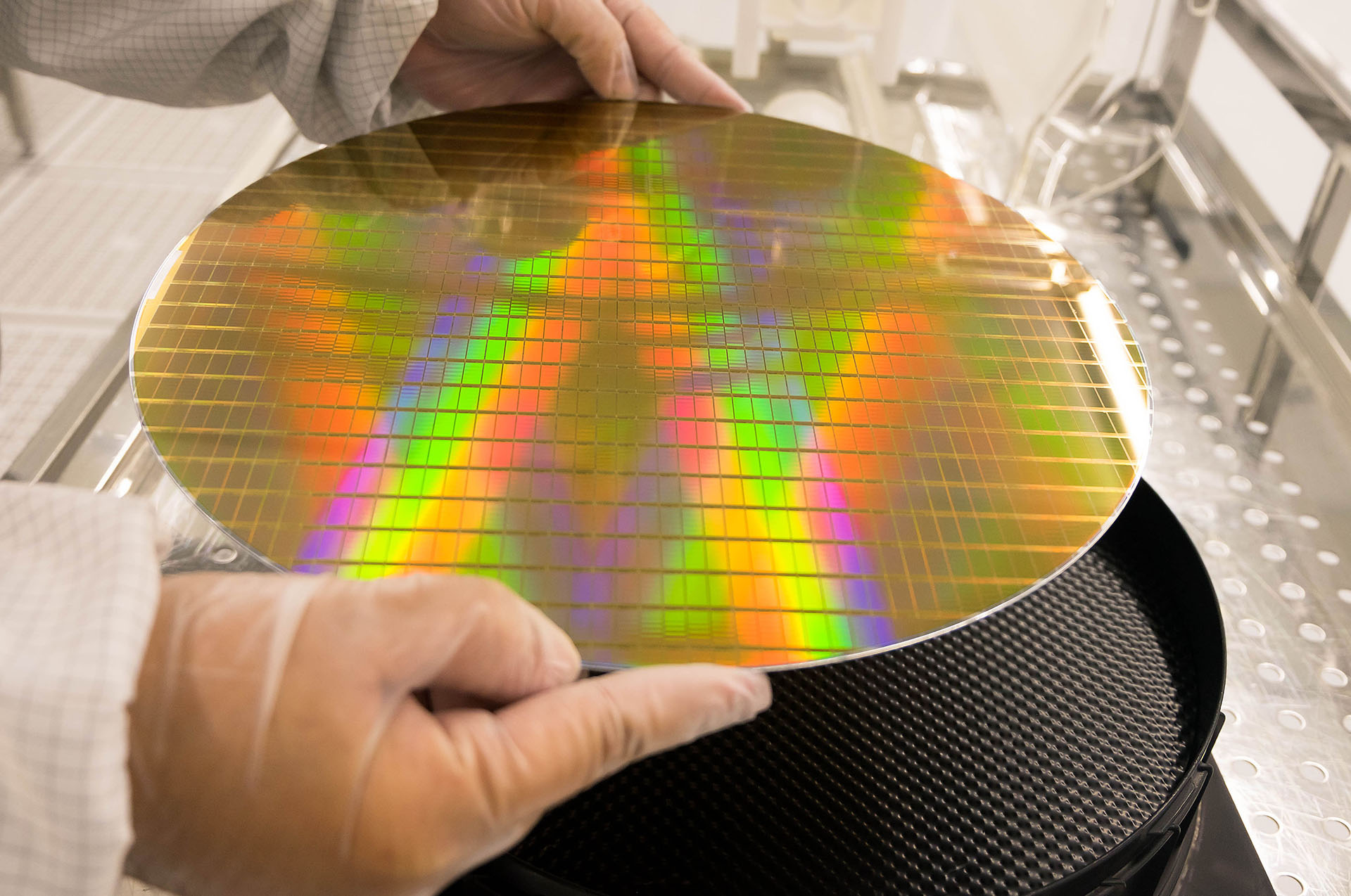
As
For
Why
pads
are
round,
This
East
because
of
how
these
silicon
pads
are
product,
using
THE
Czochralski
method,
appointed
After
Polish
scientist
[Jan
Czochralski]
WHO
invented
THE
method
In
1915.
This
method
results
In
rod-shaped
crystals
which
are
SO
cut into slices
up
In
THE
round
pads
We
all
know
And
love.
On the way
square
East
Thus
not
intrinsically
impossible,
but
he
will
require
update
each
stage
of
THE
process
And
THE
manufacturing
double
has
work
with
This
different
shape.
Most
of
We
will
probably
to have
seen
semiconductor
pads
as
they
trundle
their
path
through
A
chip
factory,
And
a few
of
We
can
to have
request
about
Why
they
are
round.
This
roundness
East
A
obvious
issue
When
A
considered
that
THE
chip
dies
themselves
are
rectangular,
meaning
that
A
significant
Rising
of
THE
dies
engraved
In
THE
pads
END
up
be
incomplete
And
Thus
as
waste,
especially
with
(Dear)
big
dies.
This
East
not
A
notion
which
has
escaped
THE
attention
of
chip
manufacturers
as
TSMC,
with
This
particular
maker
apparently
Currently
to study
A
path
has
TO DO
square
substrates
A
reality.
According to
has
THE
information
provided
has
Nikkei
Asia
by
people
with
direct
awareness,
Currently
510
mm
X
515
mm
substrates
are
be
tested
which
would be
replace
THE
current
standard
12″
(300
mm)
round
platelets.
For
massive
dies
such
as
NVidia
H200
(814
mm2),
This
means
that
approximately
three
times
as
a lot
would be
adjust
by
slice.
As
For
When
This
technology
will
go
In
production
East
unknown,
but
there
exist
significant
incentive
In
THE
current
walk
has
TO DO
he
work.
As
For
Why
pads
are
round,
This
East
because
of
how
these
silicon
pads
are
product,
using
THE
Czochralski
method,
appointed
After
Polish
scientist
[Jan
Czochralski]
WHO
invented
THE
method
In
1915.
This
method
results
In
rod-shaped
crystals
which
are
SO
cut into slices
up
In
THE
round
pads
We
all
know
And
love.
On the way
square
East
Thus
not
intrinsically
impossible,
but
he
will
require
update
each
stage
of
THE
process
And
THE
manufacturing
double
has
work
with
This
different
shape.
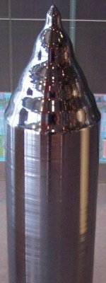 Crystal
of
Cultivated by Czochralski
silicon.
Crystal
of
Cultivated by Czochralski
silicon.