DIY laser for metal ablation
For those looking to go beyond perfboard through-hole construction for their PCBs, a PCB is usually the next step. Allowing for things like surface mount components, multilayer boards, and a wider range of parts, they're much more versatile, but have a slight downside in that they're a bit more difficult to manufacture. There are however many methods to produce them at home or in a maker space, and although we have seen many methods for their production like toner transfer, photoresist and CNC milling, it is also possible to craft them using laser ablation, although you do need a special laser to do this job.
The problem with cutting copper is that it reflects infrared, so a higher wavelength blue laser is used instead. And because you want to ablate copper, but not melt surrounding areas or cut directly through the board, extremely short, high-powered pulses are the way to go. Here, the [Munich Fab Lab] uses 9 kW pulses of about 30 microseconds each. With these specs, the copper is removed from the surface of the board, resulting in fine detail on the order of about 20 µm, which is fine enough for just about any circuit board printed. The design of the laser head itself is worth seeing.
Apart from the laser, the rest is standard CNC machine fodder, but with an emphasis on proper safety for a tool in a shared workspace, and the entire project is released under a license open and provides an affordable solution for larger-scale PCB production with extremely fine resolution and without the need for chemical quantities for the most common PCB production methods. There's a lot more information available on the project's webpage and its GitHub page as well.
Of course there are other laser based PCB production methods if you have a 20W fiber laser.
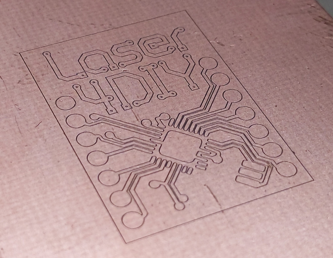
What's Your Reaction?