Suitable decoupling capacitors
If you've been building circuits for a while, you probably know that you need decoupling capacitors to keep your circuits stable. But even though it's one of our favorite techniques, scattering a few around your PCB and hoping for the best isn't necessarily the best approach. If you want to dig deeper into the why and how of decoupling, check out [Stephen Fleeman's] post on the subject.
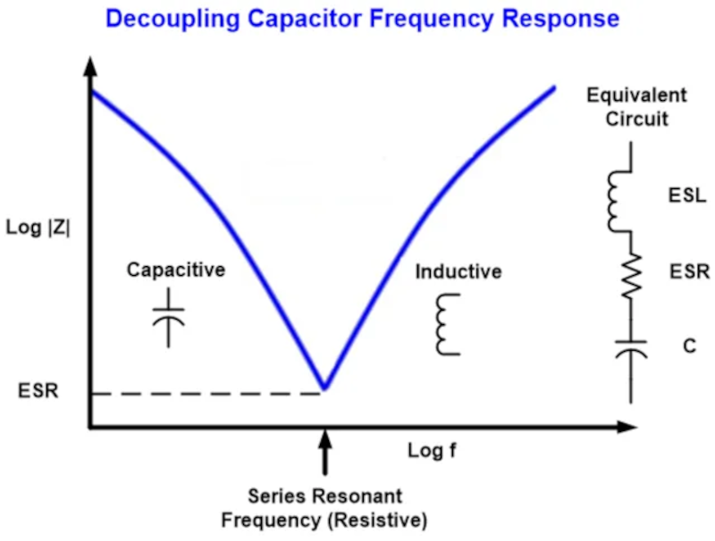
It's easy to think of capacitors as DC open circuits and high frequency short circuits, bringing noise to ground. But the truth is more complex than that. Parasitic resistance and inductance means that your simple decoupling capacitor will have a resonant frequency. This limits high frequency protection, so you often see multiple values used in parallel to respond to different frequencies.
Because parasitic resistance and inductance play a role, you can use larger traces - less resistance - and shorter runs for less inductance. Of course, you can also use power and ground planes on the PCB as a form of decoupling. At the end of the article, [Stephen] talks a bit about the importance of digital and analog terrains interacting in a specific way.
If you want to do some empirical testing, you can create a testbed and do the job. Or check with [Bil Herd] about PCB inductance.
If you've been building circuits for a while, you probably know that you need decoupling capacitors to keep your circuits stable. But even though it's one of our favorite techniques, scattering a few around your PCB and hoping for the best isn't necessarily the best approach. If you want to dig deeper into the why and how of decoupling, check out [Stephen Fleeman's] post on the subject.
It's easy to think of capacitors as DC open circuits and high frequency short circuits, bringing noise to ground. But the truth is more complex than that. Parasitic resistance and inductance means that your simple decoupling capacitor will have a resonant frequency. This limits high frequency protection, so you often see multiple values used in parallel to respond to different frequencies.
Because parasitic resistance and inductance play a role, you can use larger traces - less resistance - and shorter runs for less inductance. Of course, you can also use power and ground planes on the PCB as a form of decoupling. At the end of the article, [Stephen] talks a bit about the importance of digital and analog terrains interacting in a specific way.
If you want to do some empirical testing, you can create a testbed and do the job. Or check with [Bil Herd] about PCB inductance.
What's Your Reaction?