Using electron beams to draw tiny shapes on silicon
Over the past few years, we've seen several impressive projects where people were trying to make integrated circuits using hobbyist tools. One of the most complex parts of this process is lithography: the step in which shapes are drawn on a silicon wafer. There are a couple of ways to do it, all of them rather complicated, but [Zachary Tong] at Breaking Taps managed to make one of them work quite well. He shares the results of his electron beam lithography experiments in his latest video (embedded below).
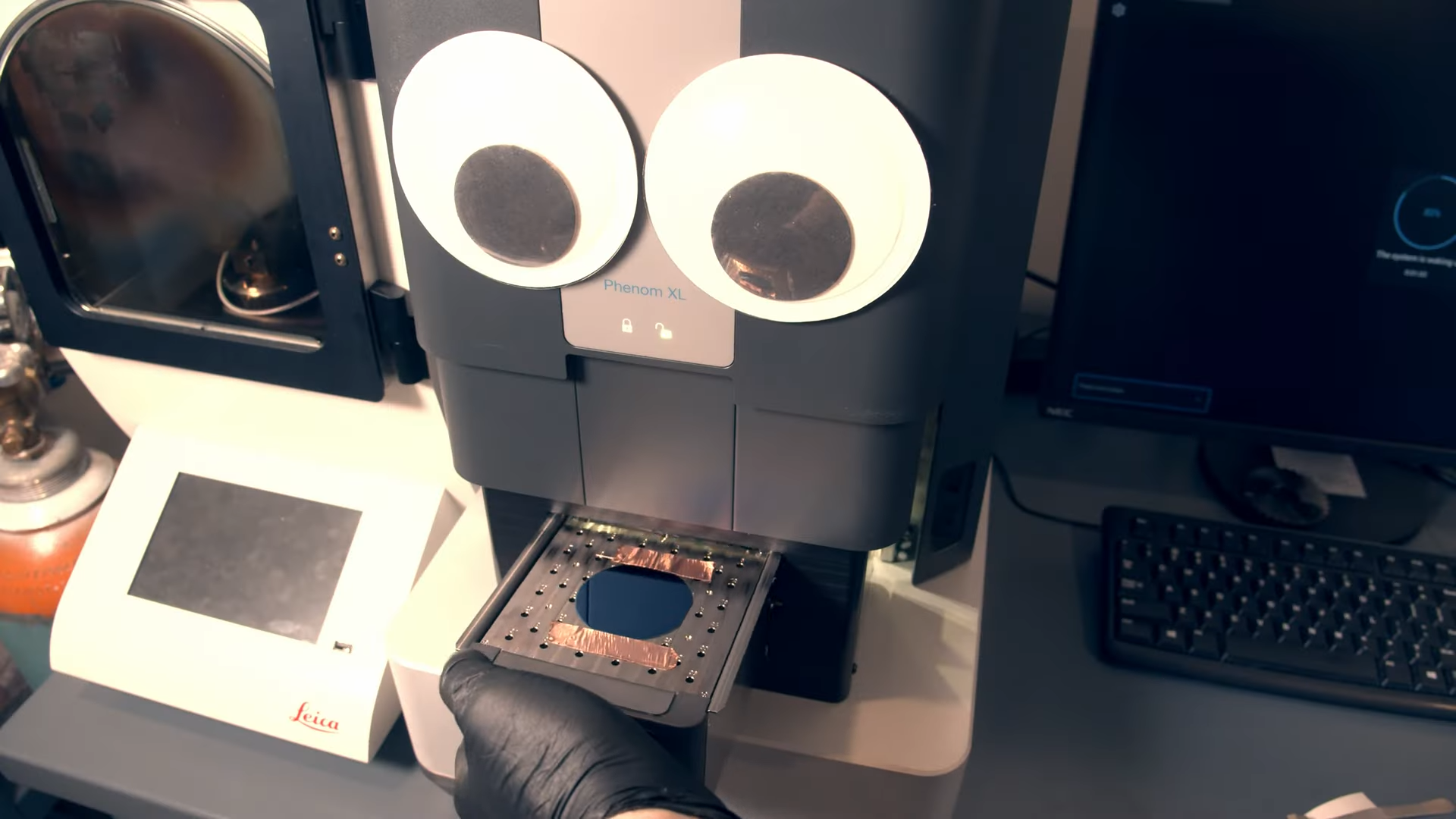
In electron beam lithography, or EBL, shapes are drawn onto a wafer using a beam of electrons in a vacuum chamber. It is a slow process compared to optical lithography, as used in mass production, but it is reasonably simple and very flexible. [Zach] decided to use his electron microscope as an electron beam lithography machine; although it is not designed for lithography, it has the same basic components as a real EBL machine and can be used as a substitute with some software adjustments.
 [Zach] also has an atomic force microscope, which he used to make these beautiful images.
[Zach] explains the whole process in detail in his video, including how he set all the parameters such as resist thickness, beam strength, exposure time and flash time. development, as well as the software tricks necessary to persuade the microscope to function as a lithographic machine. In its best runs, it managed to draw lines that were around 100 nanometers wide, which is really impressive for such a simple setup.
These electron beam lithography experiments follow [Zach]'s earlier research using lasers. Homebrew IC expert Sam Zeloof has also used electron beams in his work. Thanks for the tip, [smellsofbikes]!
Over the past few years, we've seen several impressive projects where people were trying to make integrated circuits using hobbyist tools. One of the most complex parts of this process is lithography: the step in which shapes are drawn on a silicon wafer. There are a couple of ways to do it, all of them rather complicated, but [Zachary Tong] at Breaking Taps managed to make one of them work quite well. He shares the results of his electron beam lithography experiments in his latest video (embedded below).
In electron beam lithography, or EBL, shapes are drawn onto a wafer using a beam of electrons in a vacuum chamber. It is a slow process compared to optical lithography, as used in mass production, but it is reasonably simple and very flexible. [Zach] decided to use his electron microscope as an electron beam lithography machine; although it is not designed for lithography, it has the same basic components as a real EBL machine and can be used as a substitute with some software adjustments.
[Zach] also has an atomic force microscope, which he used to make these beautiful images.[Zach] explains the whole process in detail in his video, including how he set all the parameters such as resist thickness, beam strength, exposure time and flash time. development, as well as the software tricks necessary to persuade the microscope to function as a lithographic machine. In its best runs, it managed to draw lines that were around 100 nanometers wide, which is really impressive for such a simple setup.
These electron beam lithography experiments follow [Zach]'s earlier research using lasers. Homebrew IC expert Sam Zeloof has also used electron beams in his work. Thanks for the tip, [smellsofbikes]!
What's Your Reaction?